PN Junction diode:
If one side of a single crystal of pure semiconductor (Ge or Si) is doped with acceptor impurity atoms and the other side is doped with donor impurity atoms, a PN junction is formed as shown in Fig. P region has a high concentration of holes and N region contains a large number of electrons.

As soon as the junction is formed, free electrons and holes cross through the junction by the process of diffusion. During this process, the electrons crossing the junction from N-region into the P region recombine with holes in the P-region very close to the junction. Similarly holes crossing the junction from the P-region into the N-region, recombine with electrons in the N-region very close to the junction. Thus a region is formed, which does not have any mobile charges very close to the junction. This region is called depletion region. In this region, on the left side of the junction, the acceptor atoms become negative ions and on the right side of the junction, the donor atoms become positive ions (Fig).
Forward biased PN junction diode:
When the positive terminal of the battery is connected to P-side and negative terminal to the N-side, so that the potential difference acts in opposite direction to the barrier potential, then the PN junction diode is said to be forward biased.
- When the PN junction is forward biased (Fig), the applied positive potential repels the holes in the P-region, and the applied negative potential repels the electrons in the N-region, so the charges move towards the junction.
- If the applied potential difference is more than the potential barrier, some holes and free electrons enter the depletion region.

- Hence, the potential barrier, as well as the width of the depletion region, is reduced. The positive donor ions and negative acceptor ions within the depletion region regain electrons and holes respectively.
- As a result of this, the depletion region disappears and the potential barrier also disappears. Hence, under the action of the forward potential difference, the majority charge carriers flow across the junction in opposite direction and constitute current flow in the forward direction.
Reverse biased PN junction diode
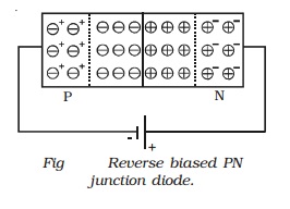
When the positive terminal of the battery is connected to the N-side and negative terminal to the P-side, so that the applied potential difference is in the same direction as that of barrier potential, the junction is said to be reverse biased.
- When the PN junction is reverse biased (Fig), electrons in the N region and holes in the P-region have attracted away from the junction.
- Because of this, the number of negative ions in the P-region and positive ions in the N-region increases. Hence the depletion region becomes wider and the potential barrier is increased.

- Since the depletion region does not contain majority charge carriers, it acts as an insulator. Therefore, no current should flow in the external circuit.
- But, in practice, a very small current of the order of few microamperes flows in the reverse direction. This is due to the minority carriers flowing in the opposite direction.
- This reverse current is small because the number of minority carriers in both regions is very small. Since the major source of minority carriers is, thermally broken covalent bonds, the reverse current mainly depends on the junction temperature.
Symbol of a semiconductor diode:
The diode symbol is shown in Fig. The P-type and N-type regions are referred to as P-end and N-end respectively. The arrow on the diode points the direction of conventional current.


