

Junction transistor
A junction transistor is a solid-state device. It consists of silicon or germanium crystal containing two PN junctions. The two PN junctions are formed between the three layers. These are called base, emitter and collector:
- Base (B) layer: It is a very thin layer; the thickness is about 25 microns. It is the central region of the transistor.
- Emitter (E) and Collector (C) layers: The two layers on the opposite sides of B layer are emitter and collector layers. They are of the same type of the semiconductor.
An ohmic contact is made to each of these layers. The junction between emitter and base is called emitter junction. The junction between collector and base is called collector junction.
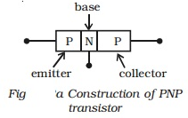

In a transistor, the emitter region is heavily doped, since emitter has to supply majority carriers. The base is lightly doped. The collector region is lightly doped. Since it has to accept majority charge carriers, it is physically larger in size. Hence, emitter and collector cannot be interchanged.
The construction of PNP and NPN transistors are shown in Fig.a and Fig.b respectively.
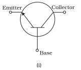

For a transistor to work, the biasing to be given is as follows:
- The emitter-base junction is forward biased, so that majority charge carriers are repelled from the emitter and the junction offers very low resistance to the current.
- The collector-base junction is reversing biased so that it attracts majority charge carriers and this junction offers a high resistance to the current.